SMART MOLDED STRUCTURES BRING SURFACES TO LIFE
Text, photos published with permission by Tactotek Oy
Further information: Tua Takkinen, Tactotek Oy tua.takkinen@tactotek.com
Authors: Outi Rusanen, Tuomas Heikkilä, Mikko Heikkinen, Paavo Niskala, Tomi Simula
This paper introduces IMSE™ technology that enables smart molded structures. (IMSE stands for Injection Molded Structural Electronics.) Smart molded structures are made by integrating and encapsulating printed electronics and standard electronic components within durable, 3D injection-molded plastics. IMSE technology and processing differs significantly from conventional electronics where components are reflow soldered onto printed-circuit-boards. We describe differences and share also some results from our reliability testing.
Introduction to IMSE Technology and Manufacturing
IMSE technology enables design innovation by integrating electronic functions into 3-dimensional injection molded plastic structures. Features, such as controls, sensors, illumination and communications, are embedded in thin 3D structures with plastic, wood and other surfaces (Figure 1).
Figure 1 – IMSE can also have natural surface finishes.

The structures are light, thin and durable. In conventional use cases, such as an in-vehicle control panel, a single part replaces a multi-part conventional electronics structure and eliminates labor-intensive electro-mechanical assembly. The part also weighs less and is significantly thinner. TactoTek has demonstrated structural electronic designs with 70% weight and 90% thickness reduction when compared with conventional multi-part assemblies (Figure 2).

Core manufacturing processes for IMSE are printing, surface mounting, forming and injection molding (Figure 3). Taken individually, these processes are mature and we use standard equipment suitable for mass production. However, the standard processes are combined in a unique way during manufacturing of IMSE.

Printing is the first core manufacturing process. Electronics and decoration (graphic inks) are printed onto plastic film or another suitable substrate material. Electronics are typically printed using silver (Ag) conductive inks and dielectric inks to insulate between layers of circuitry. The outputs are two kinds of films: electronic and surface. The latter films are used for decorations, such as icons for human-machine interface. In some cases, a single film can be used for both decoration and electronics. Both films can also be substrate for electronics.
IMSE structures have printed conductors and contact pads on polymer film. Polymer film shrinkage during subsequent processes cannot be fully controlled. The printing process minimum feature sizes are also larger than in printed circuit boards. Thus, component packages do not need small pitches. For example, ideal contact spacing is 500 𝜇m or more. Ideal contact pad area is 500 𝜇m x 300 𝜇m or larger.
Surface mounting technology (SMT) is the second core process. Components are placed and bonded, mechanically and electrically, onto electronic films. The output is 2D (two-dimensional) film substrate with components. IMSE structures use conductive and structural adhesives for component bonding instead of solder paste (Figure 4). Adhesive bonding has lower processing temperatures than reflow soldering with tin-silver-copper (SAC) solders.
Forming is the third core process. Two-dimensional electric and graphic films are thermoformed into three-dimensional shape and trimmed as needed. Outputs are 3D electric films with components and 3D graphic films. Forming is not used in conventional electronics manufacturing. TactoTek uses a high-pressure thermoforming process. During forming, component packages are subjected to elevated temperatures and pressures. The maximum temperature depends on the polymer film and is typically below 150 C. Maximum pressure is typically below 8 MPa (80 bar).
Injection molding is the fourth core manufacturing process. Three-dimensional electric films and 3D graphic films are used as inserts in an injection molding tool, and plastic resin, such as polycarbonate (PC) is injected between the films resulting in a single molded part. The output is a strong and durable structure in which electronics are encapsulated within the molded plastic. Figure 4 illustrates the material stack. Injection molding is not used in conventional electronics manufacturing, either. Some molding temperatures are higher than peak temperature during reflow soldering of SAC-solders. In addition, heat transfer during injection molding is through conduction. Thus, heat transfer is more efficient than during reflow soldering. Maximum pressures during injection molding are around 100 MPa (1000 Bar).
IMSE manufacturing often includes also pre-assembly and final assembly of control electronics. However, these processes are not specific to IMSE.

IMSE technology differs significantly from conventional electronics. Currently most electronic components are optimized for conventional electronics manufacturing that does not anticipate the temperature and pressure exposure of thermoforming and injection molding processes. Thus, TactoTek has defined criteria for ideal component packages. TactoTek also certifies all electronic components that are embedded inside injection molded polymers. [1]
Comparing IMSE Electric Films and Printed Circuit Boards
We can say that IMSE electric films are similar to printed circuit boards (PCB) because both include a substrate with conductors and surface mounted components (Figure 5). However, printed conductor traces in IMSE differ from solid copper traces in PCBs. The key-differences is that conductive inks do not conduct electricity as well as solid materials. Thus, printed conductor traces in IMSE have much higher electrical resistance than PCB traces. The 3D shape is the motivation for using conductive inks in IMSE technology. We can stretch and bend conductive inks on 3-dimensional surfaces without breaking electrically conductivity.

TactoTek way to make multiplayer structures in IMSE is also different than in PCBs. IMSE multilayer designs have several conductive layers on top of each other and there is dielectric layer between each conductive layer (Figure 6). We print the dielectric layers only to locations where traces cross each other.
Reliability Testing Results
The results presented here are part of the Certification Process for Type1-LED that was tested using an internal certification platform, Figure 7. Each certification platform contains 48 Type1-LEDs. We have surface mounted some of the Type1-LEDs on top of small radius 3D-curves. This is against our design guidelines but we wanted to push the limits of the technology and gain understanding on potential failure modes under adverse conditions. Figure 8 shows a summary of the tests and sample sizes.


At the end of the reliability tests, we checked the functionality of the Type1-LEDs. The Rapid Change of Temperature test did not cause any Type1-LED failures, all of the 480 Type1-LEDs were functional after 1000 cycles between -40 ◦C and +85 ◦C. Steady-state temperature-humidity (85◦C/85%RH) caused one Type1-LED to fail. The failed LED was in a certification platform that had been powered on during testing. The other 479 Type1-LEDs were functional after 1000 hours of elevated temperature and humidity. We also measured light luminance and color coordinates from some of the tested Type1-LEDs. Reliability testing did not cause any adverse effects.
Physical Failure Analysis Results from Type1- LED
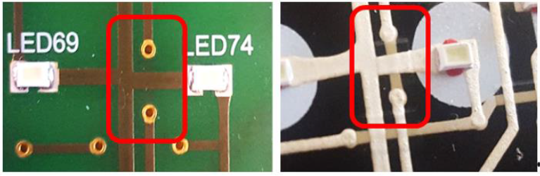
Electrical measurements indicated that the failed Type1-LED had a component internal short-circuiting. Nevertheless, we made a cross-section of the failed component because it had been mounted on top of the thermoformed 3D-curve. The cross-section showed that the component base had bent slightly. In addition, the conductive adhesive bond on one side had partly delaminated, Figure 9. As stated before, component mounting to 3D-curves with small radius is against our design guidelines.

Extended Reliability Testing Results
Testing until failure is useful for better understanding IMSE reliability. That is why we tested one of TactoTek demonstrator products for 3000 cycles in the change of temperature test. The demonstrator product, shown in Figure 10, contains 20 pieces of Type2-LEDs. Figure 11 shows summary of the tests and sample sizes.


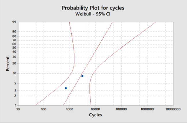
Two Type2-LEDs failed during 3000 cycles. Failures occurred at 702 and at 2988 cycles. When we fit this data into a Weibull distribution, we predict 50 percent failure point at over 10000 cycles, Figure 12. Such a high value demonstrates the reliability of the technology. However, the number of tested components was small in the extended reliability testing. Thus, we have subjected more certification platforms to extended reliability testing.
Physical Failure Analysis Results from Failed Type2-LED
We performed cross-section and scanning-electron-microscope (SEM) analysis on a failed Type2-LED. It showed that the failure mode is a fracture in the conductive adhesive used for surface mounting the component to the electronic film, Figure 13. The failure mechanism is conductive adhesive creep caused by thermo-mechanical stresses during thermal cycling.

Conclusions
TactoTek has demonstrated IMSE designs with 70 % weight and 90 % thickness reduction when compared with conventional multi-part assemblies. IMSE is also a reliable technology. The tested certification platforms and demonstrator products endured thermo-mechanical stresses and elevated temperature-humidity. Injection molding resin strengthens the structures and also protects electronics from environmental conditions, such as moisture, dust and mechanical impacts.
Acknowledgements
The authors thank Tuomas Kallio, Antti Keränen, Pasi Korhonen, Dave Rice and Johannes Soutukorva for their much-valued contribution to this work.
References
- T. Simula et al, “Component Packages for IMSE (Injection Molded Structural Electronics),” in Proceedings of NordPac, Oulu, Finland, 2018.